ASUS GeForce GTX 560 DC2 TOP review index
- Page 1 – ASUS GTX 560 DC2 TOP: Presentation
- Page 2 – ASUS GTX 560 DC2 TOP: Features
- Page 3 – ASUS GTX 560 DC2 TOP: OpenGL Tests
- Page 4 – ASUS GTX 560 DC2 TOP: Direct3D Tests
- Page 5 – ASUS GTX 560 DC2 TOP: Gaming Tests
- Page 6 – ASUS GTX 560 DC2 TOP: Power Consumption and Overclocking
- Page 7 – ASUS GTX 560 DC2 TOP: Conclusion
6 – ASUS GeForce GTX 560: Power consumption, temperature and overclocking
To measure the power consumption of the GTX 560, I used a wattmeter connected between the wall outlet and the PSU. I used FurMark 1.9.0 to stress test the GPU.
At idle state, the total power consumption of the testbed is 102W and the GPU temperature is 32°C.
The total power consumption of the testbed stressed by FurMark (1920×1080 fullscreen, burn-in mode checked) is 338W, while the GPU temperature reaches 85°C. Look at this nice temperature curve:
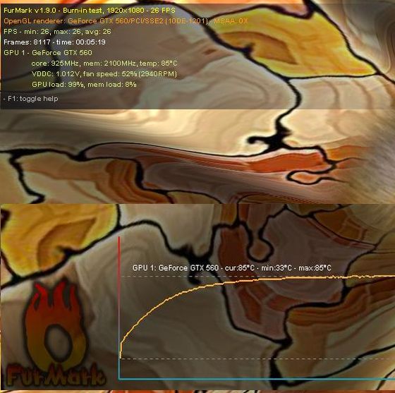
Like for the GTX 560 Ti, ASUS has not implemented the hardware power limiter we can find on the GTX 580. That explains the natural evolution of the GPU temperature.
We can the calculate the power consumption of ASUS’s GTX 560 with default GPU clock. The Corsair AX1200 PSU has an efficiency factor of around 0.9 (see this article, there is a graph of the AX1200 efficiency).
P = (338-102) * 0.9
P = 212 Watts
225W is rather far from the TDP of 160W. It’s normal. The TDP is not the max power consumption of the card (it’s rather the power draw under gaming situation) and ASUS’s GTX 560 is factory-overclocked. Then a GTX 560 with an overclocked GPU stressed by FurMark can exceed without problem 210 watts.
Here is a comparative table of the power consumption of the card ALONE (not the total power consumption of the system):
| Power: 378W – EVGA GTX 580 SC (core: 870MHz, Vcore:1.125V) – OC settings |
| Power: 330W – ASUS ENGTX580 (core: 871MHz, Vcore:1.088V) – OC settings |
| Power: 324W – EVGA GTX 580 SC (core: 797MHz, Vcore:1.082V – default settings) |
| Power: 298W – ASUS Radeon HD 6950 (core: 840MHz, Vcore: 1.300V) – OC settings |
| Power: 290W – ASUS ENGTX580 (default settings) |
| Power: 276W – SAPPHIRE Radeon HD 6970 (core: 940MHz, Vcore: 1.175V) – OC settings |
| Power: 272W – ASUS Radeon HD 6950 DirectCU II (core: 950MHz, Vcore: 1.150V) |
| Power: 272W – EVGA GTX 480 |
| Power: 260W – SAPPHIRE Radeon HD 6970 (core: 880MHz, Vcore: 1.175V) |
| Power: 237W – ASUS ENGTX570 DirectCU II (core: 742MHz, Vcore:0.950V) |
| Power: 225W – ASUS ENGTX560 Ti DirectCU II TOP (core: 900MHz, Vcore:1.025V) |
| Power: 220W – SAPPHIRE Radeon HD 6870 (core: 1000MHz, Vcore: 1.300V) – OC settings |
| Power: 212W – ASUS ENGTX560 DirectCU II TOP (core: 925MHz, Vcore: default) |
| Power: 204W – ASUS Radeon HD 6950 DirectCU II (core: 810MHz, Vcore: 1.100V) |
| Power: 197W – ASUS Radeon HD 6950 (core: 810MHz, Vcore: 1.100V) |
| Power: 185W – ATI Radeon HD 5870 |
| Power: 155W – SAPPHIRE Radeon HD 6870 (core: 900MHz, Vcore: 1.175V) |
| Power: 147W – ASUS EAH6870 |
| Power: 135W – MSI N460GTX Cyclone 768D5 OC |
| Power: 81W – ASUS GeForce GT 440 @ 823MHz |
ASUS’s GTX 560 DC2 TOP has a GPU OC-ed at 925MHz. But what is the power draw of a GTX 560 with reference clock speed? I downclocked with MSI Afterburner the GPU at 810MHz. The difference between 925 and 810 is 115MHz and that represents an extra OC of 14%.
At 810MHz, I did a FurMark burn-in test:
– total power consumption of the testbed: 319W
– GPU temperature: 81°C
I quick re-tested with 3DMark11 and FurMark 1.9.0:
– 3DMark11: P3794 @ 810MHz vs P4234 @ 925MHz : +12%
– FurMark 1.9.0: 1339 points @ 810MHz vs 1529 points @ 925MHz : +14%
The factory overclocking is impressive. But can we go further? I did a quick overclocking test: I just increased the GPU core clock without modifying the GPU voltage.
GPU@950MHz
– 3DMark11: P4310
– FurMark 1.9.0: 1565 points (26 FPS)
GPU@960MHz
– 3DMark11: P4336
– FurMark 1.9.0: 1578 points (26 FPS)
GPU@970MHz
– 3DMark11: Crash
– FurMark 1.9.0: 1595 points (26 FPS)
GPU@980MHz
– FurMark 1.9.0: crash (NV driver – OpenGL error)
You can push ASUS GTX 560 DC2 TOP GPU up to 950-960MHz which seems to be the max OC value with the default GPU voltage (VDDC). With a little bit more of voltage on the GPU, we can certainly reach 980MHz…
ASUS GeForce GTX 560 DC2 TOP review index
- Page 1 – ASUS GTX 560 DC2 TOP: Presentation
- Page 2 – ASUS GTX 560 DC2 TOP: Features
- Page 3 – ASUS GTX 560 DC2 TOP: OpenGL Tests
- Page 4 – ASUS GTX 560 DC2 TOP: Direct3D Tests
- Page 5 – ASUS GTX 560 DC2 TOP: Gaming Tests
- Page 6 – ASUS GTX 560 DC2 TOP: Power Consumption and Overclocking
- Page 7 – ASUS GTX 560 DC2 TOP: Conclusion