![]()
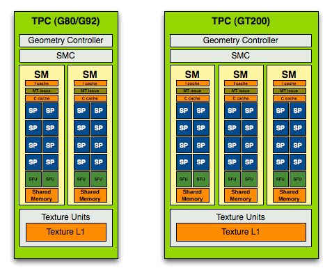
The TPC is a concept we find on NVIDIA GPUs. On G80 and GT200 architectures, a TPC, or Texture / Processor Cluster, is a group made up of several SMs, a texture unit and some logic control.
The SM is a Streaming Multiprocessor and is made up to several SPs (or Streaming Processors), several SFUs (or Special Function Unit – the unit used for transcendental functions such as sine or cosine). A Streaming Processor is also called a CUDA core (in the new Fermi terminology).
The TPC of a G80 GPU has 2 SMs while the TPC of a GT200 has 3 SMs.
G80 and GT200 TPC or Texture Processor Unit
A SP includes several ALUs and FPUs. An ALU is an arithmetical and Logical Unit and a FPU is a Floating Point Unit. The SP is the real processing element that acts on vertex or pixel data.
Several TPCs can be grouped in higher level entity called a Streaming Processor Array.
In OpenCL terminology, a SM is called a Compute Unit or CU.
But in NVIDIA’s new GPU, the GF100 / Fermi, the TPC is no longer valid: only remain the SMs. We can also say that on Fermi architecture, a TPC = a SM.
In Fermi architecture, a SM is made up of two SIMD 16-way units. Each SIMD 16-way has 16 SPs then a SM in Fermi has 32 SPs or 32 CUDA cores.

Fermi / GF100 SM architecture
I’ll update this article if necessary after the release of GeForce GTX 4xx…
References:
Pingback: GeForce GTX 480 and GTX 470 More Detailed Specs - 3D Tech News, Pixel Hacking, Data Visualization and 3D Programming - Geeks3D.com