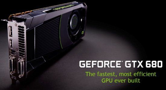
In very few days, the new high-end graphics card from the green firm will be released. Here are the latest news we can find over the Net:
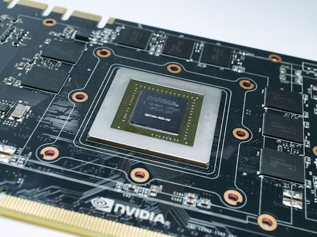
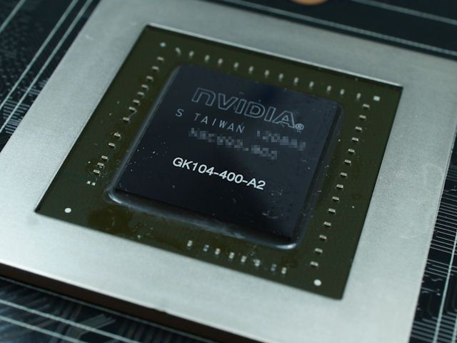
– The Kepler GK104 GPU:
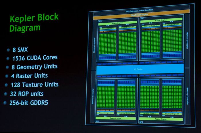
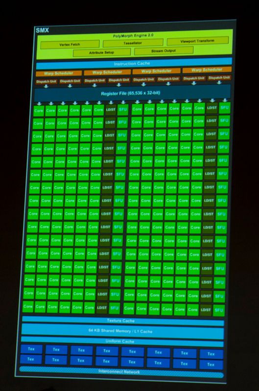
– The Kepler block diagram:
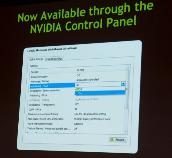
– FXAA (anti-aliasing technique) now in NVIDIA control panel:
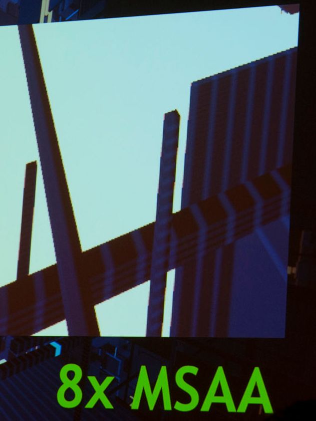
– The GTX 680 New TXAA antialiasing technique: better tah MSAA 8X, similar to MSAA 4X in terms of speed:

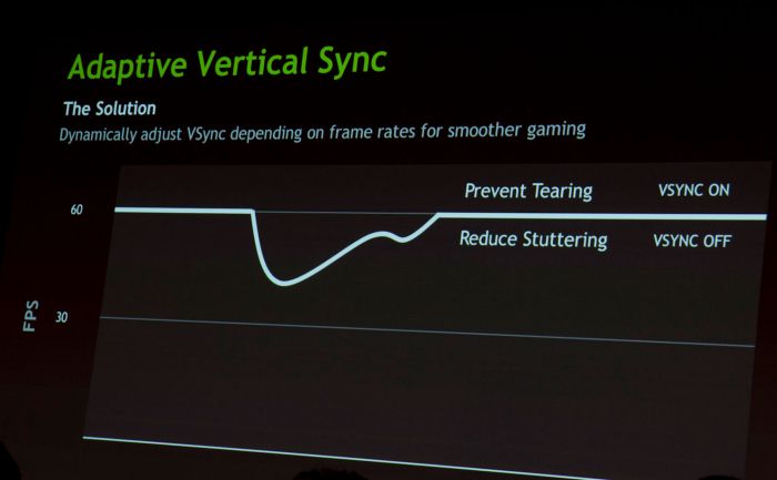
– Adaptive VSYNC (vertical synchronization):
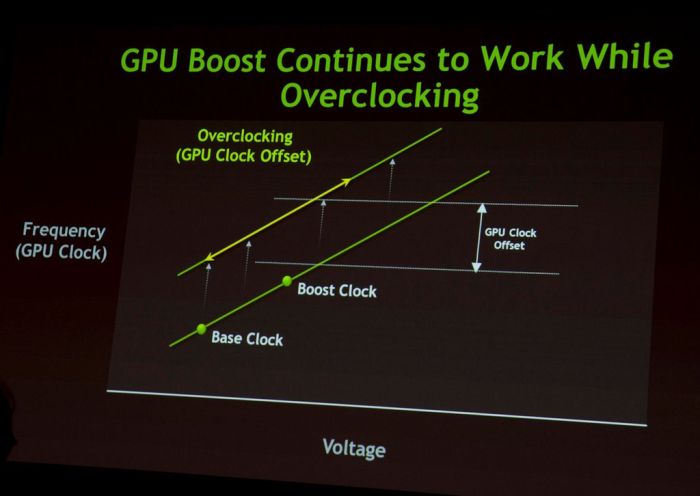
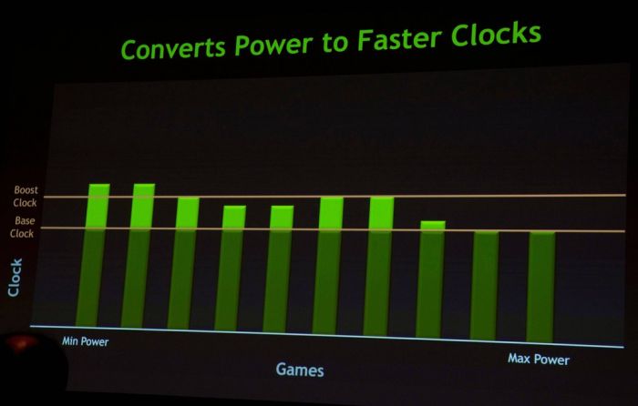
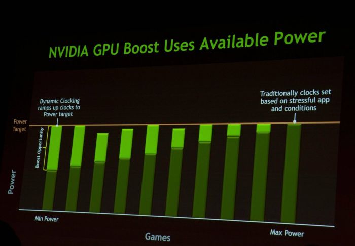
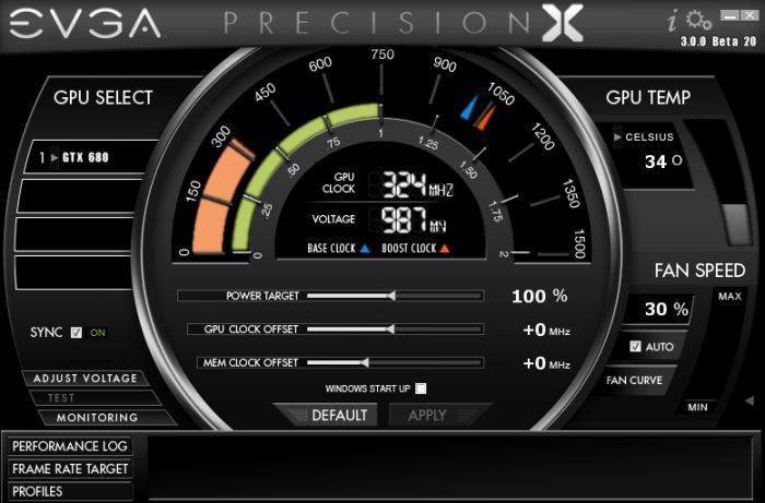
– Power management: GPU Boost and new Power functions in EVGA Precision
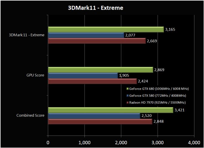
– 3DMark11: X and P score:
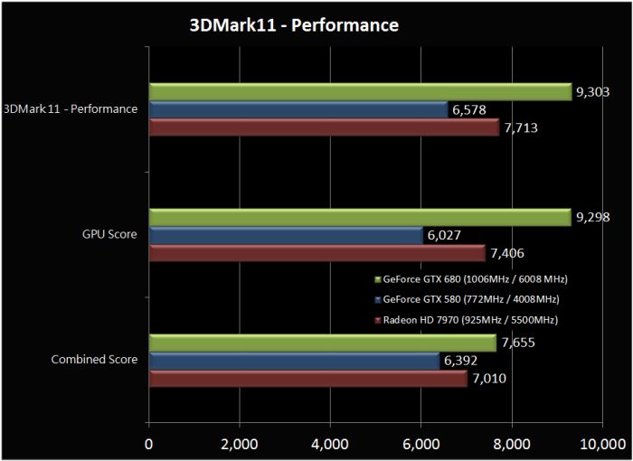
And two GTX 680 in SLI: X6243 and P16860 (source: NVIDIA GeForce GTX 680 SLI Performance Preview).
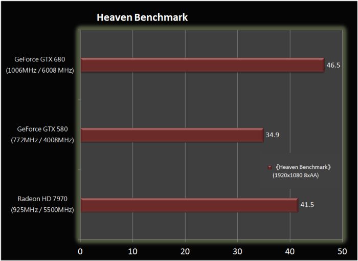
– Unigine Heaven score:
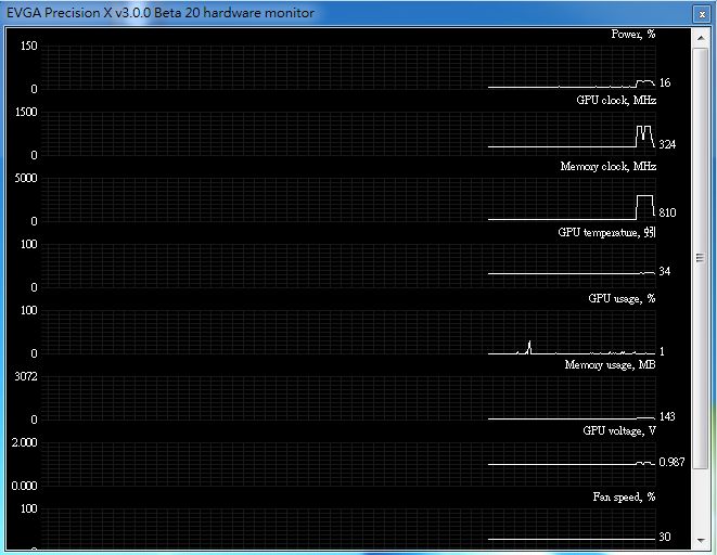
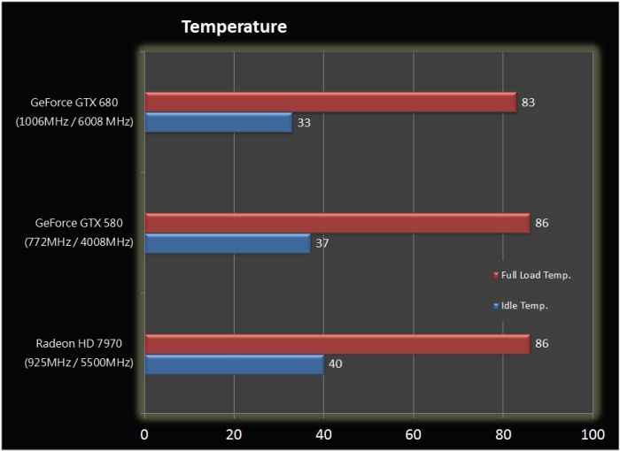
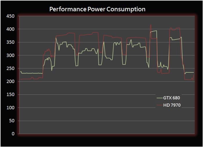
– GPU temperature and power consumption:
Related links
Interesting but it would be more interesting a comparison to a gtx 580 at the same clock speeds.
Let’s say: how will perform a gtx 680 at 772mhz core clock? 🙂
What the top connector next to the hdmi?
I don’t like GTX 680 because 680 will have crap and won’t be monster due to 195 (medium) watts, 256-bit bus and to small area of die. look benchmark war between GTX 480 and GTX 680 in 3DMark 11:
Graphics tests scores
680 – 9300 only!?
480 – 5320 😀
680 may be not good faster than 480.
I’m very happy for my GTX 480 (monster). 😛 But GK100 will be monster and might be 1.5x faster than GTX 680. 😉
Are there any informations yet about what exactly TXAA does? MSAA, CSAA, FXAA are all well documented but it seems that we have no infos yet about the inner working of TXAA…
About Adaptive VSync: That sounds alot like WGL_EXT_swap_control_tear / GLX_EXT_swap_control_tear, the OpenGL extension that Carmack suggested and implemented in Rage (after lobbying at NVidia and AMD so they implemented it in there drivers). I’d say it ‘just’ provides a switch in the control pannel to enforce this behaviour on all GL and D3D apps. That doesn’t seem like a Kepler feature (as the OpenGL extensions are available on current GPUs!).
nom, nom, nom, can’t wait for new drivers!
they changed balance again, now from ROPs to TMUs, Fermi had more ROPs less TMUs, G200 had same balance as Kepler. And they halved polymorf engine, are they just much powerful or there is something else.
Robert,
do you mean adaptive vsync could be available on previous generation of nVidia GPUs ?
Greg: As I understand adaptive vsync, it’s just a generazation of an OpenGL extension that’s actually used by Rage on current GPU (also by ATI). I don’t see why this couldn’t get included in the driver options of Fermi as well.
Hmm after all the wait I feel somewhat let down by the benchmarks, I was expecting a lot more from the 680… its almost as if this 680 scores are just the 670 midrange cards rebadged to get them out the door early.
Remember, these are first benchmarks with early drivers. Performance will improve.
trollfed:
I think the problem is that ATI launched 7970 first.
Thus NVIDIA did enough to beat it and claim ‘fastest GPU’ title instead of pushing it faster with more power and higher temps AKA the 480.
yea.. they just adapted with 7970 performance,, 10% faster is enough to claim performance crown.. ;p
So this one has 3x the shader count of 580, but still somehow has only about 20-25% gains over gtx580 ? How can this be possible, unless the new “shader processors” that come with kepler, are far more inefficient than the previous ones?
ok, to be exact, this card has 2.64 times more cuda cores than gtx580, and at best is 50% faster than gtx580 ( gpu score ). How is that even possible ?
EVGA Precision X v3.0.0 beta 20 ??!!?? LOL
I want it! where can I find ? asd…
mirror says:
“ok, to be exact, this card has 2.64 times more cuda cores than gtx580, and at best is 50% faster than gtx580 ( gpu score ). How is that even possible ?”
but only twice times more texture modules and 1.5 times less ROP units 😛
and there is only 256-bit memory, GTX580 has 384-bit memory
sigh there’s so much confusion…!
Guys, the GTX 680 is based on the GK104. That is the performance chip, not the enthusiast chip.
It seems that it turned out to be better than anticipated, or Tahiti turned out to be worse than expected, so Nvidia decided to place it higher.
The true GF110 successor will be GK100/110.
Also please don’t compare Fermi’s cuda cores, with Kepler’s cuda cores. They are quite different. There is no hotclock for one. So 1536 kepler cuda cores does not mean 3X fermi cores. Fermi’s cores where running at double the speed.
From where I’m standing, I see GK 104 being 33% faster than GF110 and GK100/110 being another 33% faster on top of that.
“ok, to be exact, this card has 2.64 times more cuda cores than gtx580, and at best is 50% faster than gtx580 ( gpu score ). How is that even possible ?”
Well, let’s look at the raw performance:
A 580 has 512 cores clocked at (e.g.) 1544MHz (twice the clock of the rest of the chip) and each core can do a multiply-add in one clock -> 512*1544*2 = 1581 GFLOPs.
Some sources say the 680 has 3TFLOPs, if that’s accurate the following would make sense:
1536 (cores) * 1006MHz * 2(mult-add) = 3090 GFLOPs!
I’d say the cores ar clocked at ‘native’ GPU clock.
‘Only’ twice the theoretical performance at 3 times the cores.
This GPU has more ALU performance, more texture units and faster texture lookup relative to the ALU speed and more SFUs per Int/Float ALU. It’s build for more complex shaders, not more FPS in games with simple shaders (not more ROPs).
http://i.imgur.com/tsQ5p.jpg
GTX 680 is very good at tessellation despite only have 8 tessellator(Polymorph Engine 2.0) units, it’s much faster than GTX 580 with 16 tessellator(Polymorph Engine 1.0) units.
I didn’t know that Kepler had a single clocked ALU domain system. Is this confirmed by NVidia?
http://i43.tinypic.com/2am93r.jpg
dominates the 7970
Corwin: A single clocked ALU is not confirmed by NV, but if you do the math (and didn’t made a mistake) this is the only explanation for
A) rumors of ‘just’ 3 TFLOPs
B) NVidia not rubbing ‘worlds first 6 TFLOP GPU’ all over AMDs face…
C) fits the current benchmarks
your calculations would make some sense ( and i would attribute the 1.5 measured from 2 theoretical difference to immature drivers ) and that’s assuming the shaders run around 1000Mhz.
http://en.wikipedia.org/wiki/Comparison_of_nvidia_gpus#GeForce_600_Series
wiki says the shaders will run around 1411Mhz. We will have to wait and see the real thing.
@mirror: DirectX not 11.1 but officially DirectX 11 only
Dare I say it but this could be the first good nVidia GPU since the G8x series. Finally not a stupid brute force approach
“Dare I say it but this could be the first good nVidia GPU since the G8x series. Finally not a stupid brute force approach”
Actually it’s quite opposite. G92, GT200 and GF100 – all of them had smarter “shader core” – less peak performance, better utilization in both rendering (shades and lights) and complex GPGPU apps. Now when AMD finally dumped their game oriented arch. to GCN (smarter, cuda like) NV goes with lots and lots of SP (harder to utilize efficiently except games). But hey, I might be wrong. We’ll see soon enough.
Very good power consumption, noise and temperature.
http://i.imgur.com/TCsiO.png
http://i.imgur.com/jbrbV.png
http://i.imgur.com/IDbS2.png
http://i.imgur.com/d2jbh.png