
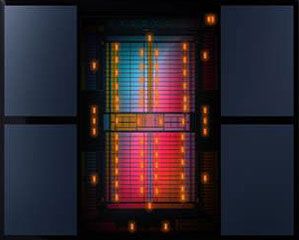
AMD has officially launched the new Radeon VII gaming graphics card. This new graphics card loves the number 7. The Radeon VII is based on the second generation of Vega architecture (Vega 2, V2, VII, 7…) and is the first graphics card with a 7nm GPU (VII, 7, …). And what’s the day number today? The 7! The Vega 20 GPU features 3840 shader cores, 64 ROPs and 240 TMUs. Compared to the Vega 1, this new GPU is built on TSMC 7nm process and comes with scientific compute and machine learning improvements.
With its 16GB HBM2, the Radeon VII is around 30% faster then the previous Radeon Vega 64 and targets NVIDIA’s GeForce RTX 2080. But according to some reviews, the RTX 2080 is, in reality, 14% faster than the Radeon VII. The real competitor is rather the old GeForce GTX 1080 Ti… The Radeon VII launch price is USD $699.
Radeon VII specifications
- GPU: Vega 20 (GCN 5), base clock: 1400MHz, boost clock: 1750MHz, process: 7nm, transistors: 13230M
- Shader cores: 3840
- Compute units: 60
- TMUs: 240
- ROPs: 64
- Memory: 16 GB HBM2 @ 1000MHz, mem bus width: 4096-bit
- FP32 TFLOPS: 13.8
- FP64 TFLOPS: 1/4 FP32
- TBP (Typical Board Power): 300W
- Power connectors: two 8-pin
- Output connectors: 3 x DisplayPort + 1 x HDMI


Junction Temperature
AMD has placed 64 thermal sensors on the GPU die. The highest reading of all these sensors is called junction temperature. The hotest spot on the GPU is used to properly clock the GPU. AMD recommends to use the new API to read the GPU temperature. Utilities like GPU-Z or GPU Caps Viewer will probably report wrong values for the GPU temperature.
Reviews
- techpowerup.com
- anandtech.com
- gamersnexus.net
- bit-tech.net
- guru3d.com
- hothardware.com
- hexus.net
- kitguru.net
- techreport.com
Video Reviews