EVGA GTX 580 Classified Ultra review index
- Page 1 – Overview
- Page 2 – Gallery
- Page 3 – Specifications
- Page 4 – OpenGL Tests
- Page 5 – Direct3D Tests
- Page 6 – Gaming Tests
- Page 7 – Power consumption and Temperature
- Page 8 – Conclusion
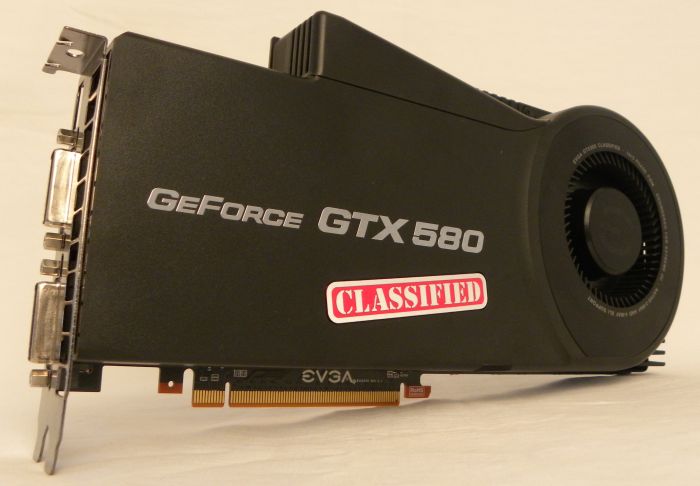
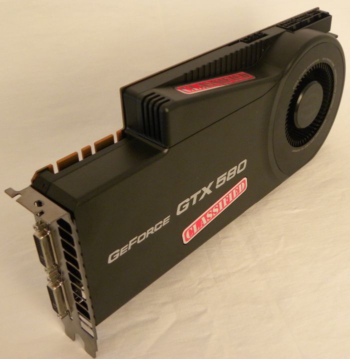
2 – EVGA GTX 580 Classified Ultra: Gallery
Here is the global view of the board:
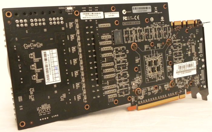
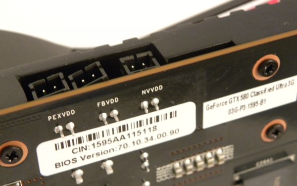
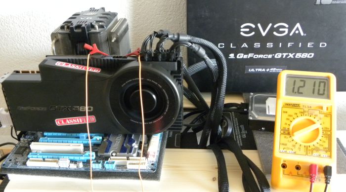
The GTX 580 Classified has three voltage check points: one for the GPU (NVVDD), one for the memory (FBVDD) and one for the PLL (PEXVDD). It’s a pity that EVGA does not provide the connectors for these check points. But if you can still connect your voltmeter to the pins on the rear side of the PCB, they are long enough.
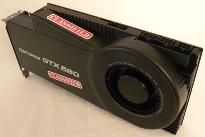
The 14+3 phase power circuitry requires many power connectors as you can see: 8-pin + 8-pin + 6-pin:
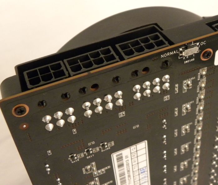
That means that the board can handle up to (75 + 2×150 + 75) = 450W.
Close to the power connectors, there is a switch that allows to switch from normal mode to OC mode. OC mode disables all kind of protections like OCP and OVP (Over Current and Voltage Protection) or overheating (source). OC mode is for extreme overclocking with liquid nitrogen (LN2). There is no longer communication between the GPU and VRM. Actually, you can use OC mode only if you have EVGA’s EVBot connected to the card via this port:
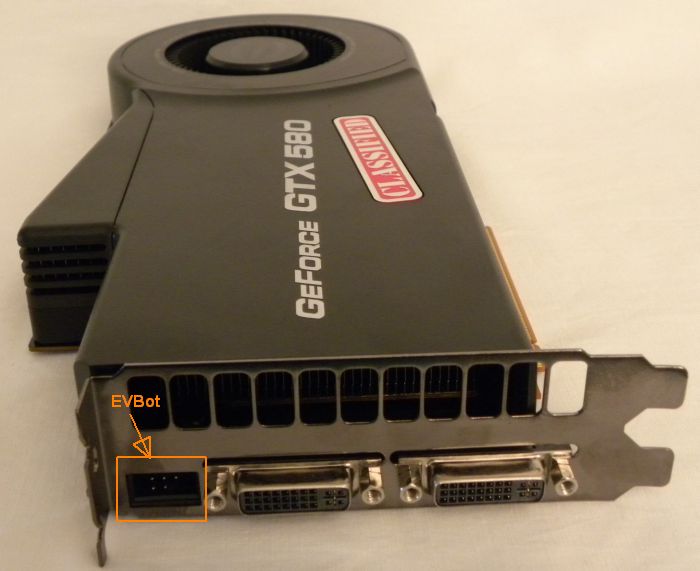
EVBot is used to control GPU voltage as well as other important paramaters. In this review, I only used the card in normal mode, which was enough!
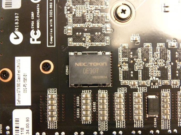
Like the Matrix GTX 580, EVGA uses a big capacitor: a NEC/Tokin Proadlizer film capacitor (Model: 0E907). This capacitor (2.5V / 900uF) is used to provide a more stable GPU voltage, which is required with high overclocking settings.
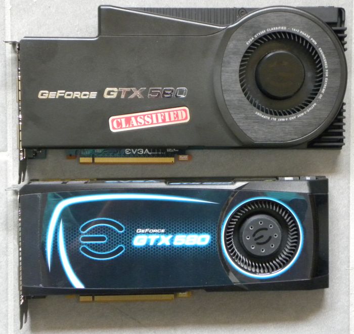
To end up the gallery, here is the regular GTX 580 side by side with the GTX 580 Classified:
EVGA GTX 580 Classified Ultra review index
Uhmm my 2 GTX 580 (model 1580 reference design) have a higher ASIC quality: 80.5 and 76.5 !
And they overclock nicely at 910/2250 @ 1.138v 24/7
They are also stable at 920 but 910 seems better to me.
(EVGA of course)